
By Jason Spruell
For over 55 years, the semiconductor industry has continued down the path of unrelenting miniaturization as described by Moore’s Law. A majority of this time has been devoted to advancing photolithographic processes to create ever-decreasing feature sizes on logic processors and memory chips. From i-line and 248 nm, to 193 and 193 immersion, and now EUV, the industry has grappled with multiple generations of photolithography technology and pondered the limits of using light-alone to achieve greater and greater transistor density. While these lithography advances continue, the rising costs of finer photolithography patterning are driving the innovation revolution in scaling of the way the chips are wired and packaged.
The advances in semiconductor packaging technologies have also evolved at a rapid pace to not only keep up with the down-scaling of integrated circuits, but to also allow for new and unique chip architectures that provide an ancillary strategy to achieving the computational power improvements outlined by Moore’s Law—an approach that is sometimes referred to as “More than Moore”.
Semiconductor packaging technologies have traditionally referred to the physical encasement of an integrated circuit—referred to as a die—within a robust protective package, that protects the semiconductor from mechanical, thermal, and electrical stress. However, as semiconductor packaging technology has evolved, it has become synonymous with the interconnection of separate device components. To this end, semiconductor packaging is integral to furnishing the inputs and outputs (I/Os) that connect each semiconductor chip to others, and ultimately to the world at large. In short, powerful electronic components of smaller size and greater functionality rely on innovative electronic packaging. These advances in semiconductor packaging technologies have enabled chip manufacturers to create unique 3-dimensional architectures that work in combination with photolithographic technologies to achieve the exponential growth charted by Moore’s Law.
A case in point is the ongoing revolution of 3D integration of modular chiplets with discrete functions into small packages through modern packaging technology. These designs are now more than concepts with commercial systems offered by Intel, Samsung, AMD, TSMC and others.
Effective and reliable wiring integration is the key to such massively interconnected package designs. Scaling of electronic packaging is achieved through the fine wiring known as redistribution layers (RDLs, Figure 1). Polyimides are essential to creating effective redistribution layer dielectrics that insulate these fine wires. The electrical, thermal, and mechanical properties of polyimides as a class of materials make them ideally suited as RDL dielectric materials.
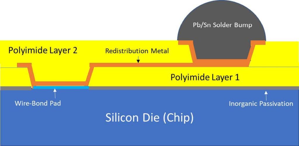
Figure 1. An enlargement displaying the PI layers (yellow) serving as insulation for the redistribution metal wiring used to contact the underlying silicon chip (die) and structural support for the entire package.
Fluorinated Monomers Create Value
The most advanced polyimides benefit from the property enhancements of fluorinated monomers. Fluorinated monomers incorporated into the polyimide backbone reduce the dielectric constant and loss factors making them better insulators for higher frequency electric signals, such as those being deployed in 5G applications. Moreover, the fluorinated monomers improve the environmental robustness of the package by reducing the moisture uptake of the polyimide. The thermal and mechanical properties of the polyimide may also be positively tuned through selection and blends of fluorinated monomers, for example fluorinated polyimides typically have lower coefficients of thermal expansion (CTE), a critical need in RDL applications.
Facile Processing is Key
The processing of the polyimide materials used in various packaging layers is also critically important. As discussed in the previous blog in this series, the traditional thermal and chemical imidization techniques have significant limitations and restrictions including high temperature requirements and restrictions on the monomer scope. By working with our partners, Halocarbon Polyisoimide Processing Agents have enabled breakthroughs to produce both non-photosensitive and photosensitive polyimides.
Fluorinated materials enable breakthroughs and enable More than Moore in electronic packaging. Contact us to learn more about how Halocarbon Electronics Solutions enables breakthroughs in polyimides or reach out directly to our sales manager.


Leave a Reply