
By Jason Spruell
Innovative technologies are driving advances in the semiconductor packaging industry resulting in exponential growth of the number input/outputs (I/Os), modular designs for greater economies of scale, thinner and smaller chip packages.
The key packaging technology is known as Fan-Out Wafer Level Packaging (FOWLP) in which the input/outputs (I/O) are “fanned-out” from the chip and spread across a wide area so as to increase I/O density. As this technology has evolved, the increase in I/Os has been coupled with the replacement of thick laminate substrates such as printed circuit boards (PCBs) with more modern ultra-thin packaging polymers. This design enables the tighter lateral integration of chips and the 3D-stacking of chips on top of one another to create integrated designs. Beyond the advantages of scale, heterogeneous integration of various types of chips and chiplets reduces energy consumption and increases the communication speeds between these components. The resultant devices are thin packages that accommodate more metal wires at tighter spacings which must be well insulated.
Packaging Materials with Strict Specifications
Significant materials requirements are exerted on the polymers that serve as the insulation between metal wires and structural elements to support the packaged chip. These polymers must have both low dielectric constant (Dk) and loss factor (Df) to serve as effective insulation between the copper I/O wires. As the electrical frequencies are increasing with the advent of 5G, the importance of low Df materials at higher frequencies is paramount, thus introducing further material requirements on the RDLs. Additionally, to prevent warping of the device, they must have very low coefficients of thermal expansion (CTE) which match the underlying silicon substrates and highly filled epoxy-mold compounds which are stacked together within the packaging. Additionally, they must have high glass transition temperatures (Tg), sufficient toughness, and moisture resistance to be reliable over the lifetime of the device.
To meet these stringent material demands, the industry has increasingly relied upon polyimides (PIs) and polybenzoxazoles (PBOs). These materials have the proper combination of the following properties to enable the application:
- Low Dielectric constant and loss factor
- Low Coefficient of Thermal Expansion (CTE)
- High Temperature stability
- Robust Mechanical properties
Each of the above properties are further enhanced using fluorinated monomers in the PI or PBO design. Halocarbon Electronics Solutions offers fluorinated materials at scale to enable these advantages and create the next breakthroughs.
Processing Demanding Innovation
Even with the best monomer formulations, processing these dielectric materials in the correct geometries for the application can be a challenge (Figure 1). For patterned applications, photosensitive polyimides (PSPI) are most often used. In the case of unpatterned layers, non-photosensitive PI layers are sufficient. In either case, lower temperature cure PIs are needed due to the limited thermal budget set by the surrounding materials, such as epoxy mold compound. Advances in cure catalyst and monomer design have led to reductions in cure temperature, however, the target of a less than 200 °C cure has been elusive for polyimides. The lower cure temperatures of PBOs have enabled their use but they suffer from high CTEs as a trade-off.
With critical needs including:
- Reducing the cure temperature
- Lowering the CTE
- Reducing the Dk and Df
- Maintaining or increasing Tg
The industry is well served through a larger palette of polyimide monomers, including some which were previously prohibited for processability reasons. Fortunately, the polyisoimide processing aid we discussed in a previous post can provide these valuable enhancements to both PSPI synthesis as well as non-photosensitive PIs.
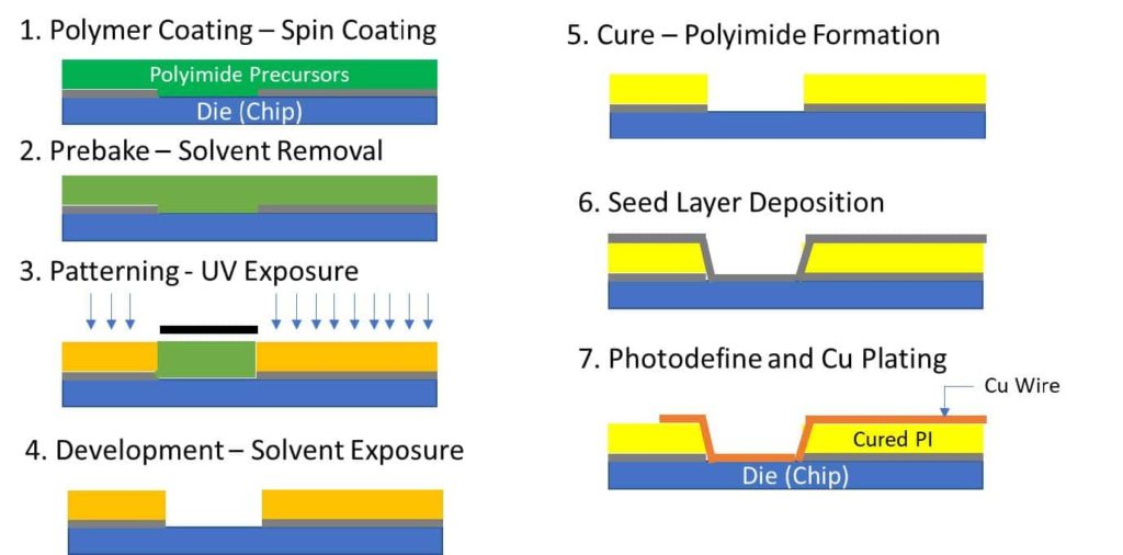
Figure 1. Multiple steps utilized to pattern and manufacture the Cu wiring insulated with the final polyimide. Utilizing a polyisoimide as the “Polyimide Precursor” can enable lower cure temperatures and larger monomer selection scope.
By adopting a polyisoimide approach enabled by the Halocarbon Polyisoimide Processing Agents to form the final polyimide, the cure temperature is reduced, and the potential monomer scope increased as we discussed in the previous blog post. Moreover, the lower viscosity and higher potential solids content of the polyisoimide solution can enable more economical application of the formulated PI solutions in the packaging tracks. Additionally, improved solubility of the polyimide precursor solution enables a broader solvent selection for the dispense solution and developer solvents used in the RDL production process. In short, by removing process limitations, the polyisoimide route widens the design scope for both monomers and solvents leading to polyimides to meet the stringent performance targets.
These modifications can thus enable lower cure temperatures, lower Dk and Df materials, low CTE materials, with reduced defectivity to drive ever finer pitches, smaller devices and enable next generation 5G packages.
The future is bright for Semiconductor Packaging
The first generation RDL devices utilized 10-15 µm metal lines. That dimension has shrunk since with the chip sets in high volume manufacturing today utilizing 5 µm lines. As the industry continues to push these dimensions lower, with 2 µm on the horizon, and the advent of multiple stacked RDL routing layers, material demands for better insulative and more easily processed RDL dielectrics are increased. These material requirements can be addressed in part using Halocarbon Polyisoimide Processing Agents.
In the next blog post, we will discuss how the Halocarbon Process Agents can be used to form more effective photosensitive, photo-definable polyimides (PSPIs) and how that technology further enables advanced electronic packaging.
Contact us to learn more about Halocarbon’s solutions for the formation of polyisoimides for electronic packaging or reach out directly to our sales manager.


Leave a Reply