With over a decade of experience, Halocarbon Electronics Solutions continues to accelerate the development of next-generation semiconductor packaging materials. By working closely with our partners, we leverage industry-wide expertise and resources to meet increasingly stringent requirements, overcoming the challenges and previously perceived limitations of the semiconductor fabrication industry. The critical role of Halocarbon Electronics Solutions in the advancement of semiconductor packaging materials enables new and unique chip architectures that achieve the ambitiously charted predictions of Moore’s Law.
What are Semiconductor Packaging Materials?
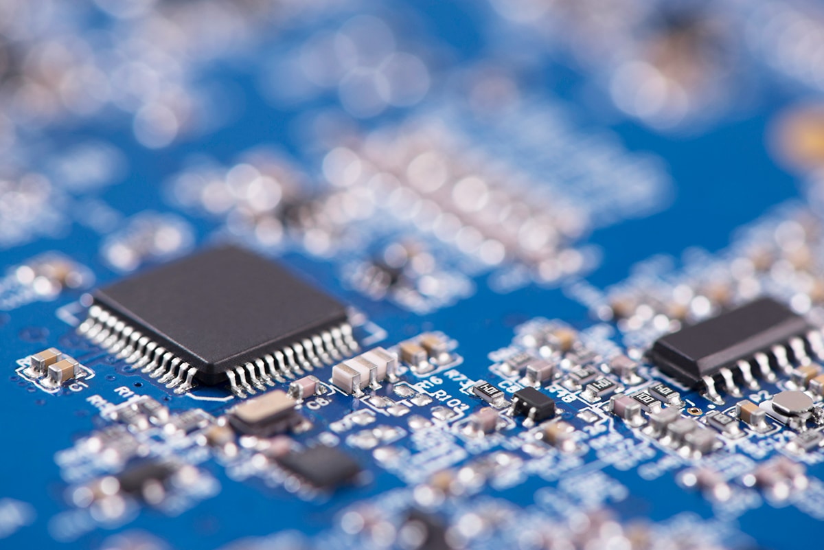
Semiconductor packaging materials are electronic solutions designed to protect semiconductor devices or integrated circuits and connect them to external environments and platforms, such as printed circuit boards (PCBs). As semiconductor packaging continues to evolve, the term no longer simply refers to the physical encasement—it has grown to embody the interconnection of device components that are integral to linking each chip to others. This class of solutions must exhibit a range of beneficial properties, including mechanical strength, chemical stability, thermal performance, and light resistance, as these characteristics are critical to the connection and performance of the semiconductor components.
Advances in Semiconductor Packaging
Modern advances in semiconductor packaging emanate from the development of innovative dielectric materials. Specifically, polyimides with excellent electrical, thermal, and mechanical properties have facilitated unprecedented package designs and capabilities. Breakthroughs in fluorochemistry and property enhancements of fluorinated monomers help to reduce the dielectric constant and loss factors, optimal for 5G technology and cutting-edge electronic components. Additionally, Halocarbon Electronics Solutions for polyimide technology contributes to both non-photosensitive and photosensitive polyimides, leading to a range of diverse semiconductor packaging materials for a myriad of applications.
Commercial-Scale Chemical Isoimidization Technology
As a recent development, a chemical isoimidization process has become the preferred process for commercial-scale polyimide production. With high-purity chemical isoimidization agents, Halocarbon Electronics Solutions offers a range of solutions that enable manufacturers to cost-effectively prepare polyamide solutions at greater concentrations. The intrinsic attributes of these high-performance agents provide an abundance of advantages for large-scale development and design, such as superior solubility, low viscosities, and broad temperature compatibility.
Photosensitive Polyimides in Semiconductor Packaging Materials
The experts at Halocarbon Electronics Solutions work closely with their partners to simplify the approach to the production of vital semiconductor packaging materials, such as photosensitive polyimides. Halocarbon Isoimidization Process Agents enable manufacturers to overcome the design and production challenges of developing photosensitive polyimides, such as costly purification to remove undesirable byproducts. The alternative and streamlined methods developed using these innovative materials ultimately support the production of thinner, smaller, and faster semiconductor packaging materials to drive the electronics industry forward.
Contact us to learn more about how Halocarbon Electronics Solutions enables breakthroughs in semiconductor packaging, or reach you directly to our sales manager.


Leave a Reply